
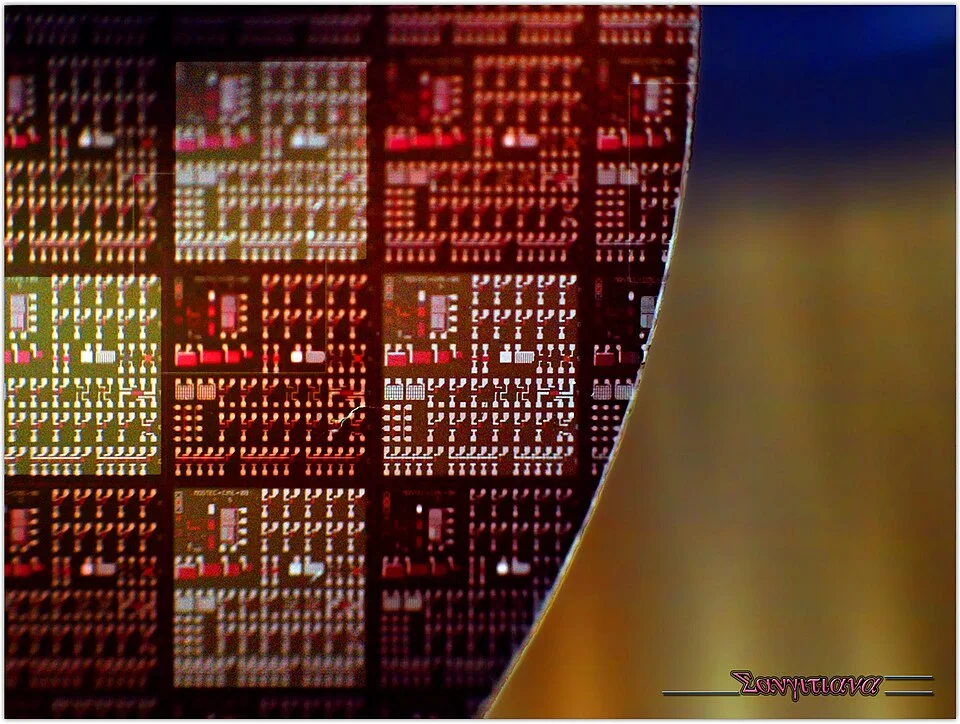
Semiconductor wafer used as a substrate for integrated circuits and other microdevices.
Credit: Sangitiana Fararano · CC BY-SA 2.0 · sourceResized and converted to WebP; uncropped.
1. Scientific foundations: bands, carriers and doping
A semiconductor has electrical properties between those of a conductor and an insulator, but its defining advantage is controllability. In solids, electrons occupy allowed energy bands. The valence band and conduction band are separated by a band gap. In semiconductors, thermal energy or absorbed light can enable some electrons to enter the conduction band, leaving holes behind. Both electrons and holes contribute to current.
An intrinsic semiconductor is a sufficiently pure material in which electron and hole concentrations are equal. Silicon and germanium are elemental semiconductors, while gallium arsenide, gallium nitride and silicon carbide are compound semiconductors. Silicon dominates because of its mature manufacturing ecosystem, abundant raw-material base and ability to form a useful insulating oxide, silicon dioxide. However, ordinary sand cannot be used directly for chips: electronic-grade silicon requires extensive purification and crystal processing.
Doping deliberately introduces small quantities of impurities. Adding pentavalent atoms, such as phosphorus, to silicon produces n-type material with electrons as majority carriers. Adding trivalent atoms, such as boron, produces p-type material with holes as majority carriers. Minority carriers remain present in both types. The labels positive and negative refer to the dominant mobile carriers, not to a net charge on the bulk material.
For intrinsic semiconductors, conductivity generally rises with temperature because additional charge carriers are generated. This contrasts with the usual behaviour of metals, whose resistance increases with temperature. In doped materials, the precise temperature dependence also depends on dopant ionisation and carrier mobility.
- A hole is a missing electron in an otherwise occupied electronic state; it behaves as a positive charge carrier.
- Semiconductors are not superconductors: superconductivity involves zero electrical resistance under specified conditions.
- Silicon and silicone are different: silicon is an element, while silicones are polymeric materials.
Timeline
1947
The first working point-contact transistor was demonstrated at Bell Laboratories.
1958–1959
Jack Kilby and Robert Noyce made foundational contributions to the development of integrated circuits.
1965
Gordon Moore published the observation that became known as Moore’s law.
December 2021
India approved the ₹76,000-crore semiconductor and display ecosystem programme.
September 2022
India modified fiscal support for semiconductor and display manufacturing.
February 2024
The Union Cabinet approved semiconductor projects at Dholera, Morigaon and Sanand.
2. Junctions, transistors and major applications
When p-type and n-type regions meet, carriers diffuse across their interface, creating a depletion region and an internal electric field. This p–n junction is the basis of many semiconductor devices. Forward bias reduces the junction barrier and permits substantial current; reverse bias ordinarily allows only a small leakage current until breakdown conditions occur. A diode therefore supports rectification, the conversion of alternating current into unidirectional current.
Transistors regulate electrical current and function as switches or amplifiers. Metal-oxide-semiconductor field-effect transistors, or MOSFETs, are foundational devices in modern integrated circuits. Complementary metal-oxide-semiconductor technology, or CMOS, combines n-channel and p-channel transistors to reduce static power consumption. An integrated circuit places interconnected electronic components on a common semiconductor substrate.
Applications extend far beyond smartphones. Logic chips execute instructions; memory chips store information; analogue chips handle continuously varying signals; and mixed-signal chips connect analogue and digital systems. Sensors detect physical changes, while power semiconductors control and convert electrical energy in electric vehicles, railway traction, renewable-energy systems and industrial equipment.
Light-emitting diodes produce light through electron–hole recombination. Photodiodes detect light, and solar cells convert incident light into electrical energy through the photovoltaic effect. Wide-band-gap materials such as silicon carbide and gallium nitride can support high breakdown fields and demanding operating conditions. Silicon carbide is important in power conversion, while gallium nitride serves power electronics and radio-frequency applications.
- DRAM is volatile memory and normally needs periodic refreshing; NAND flash is non-volatile.
- A chip need not use the smallest available process node to be commercially or strategically important.
- Many automotive, industrial and power-management applications rely on mature or specialised manufacturing processes.
Simplified chip production chain
- 1. Define chip functions and architecture
- 2. Design and verify circuits
- 3. Prepare layouts and manufacturing masks
- 4. Fabricate circuits on semiconductor wafers
- 5. Test wafers and separate individual dies
- 6. Package, conduct final testing and supply to users
3. How chips are manufactured
Manufacturing begins with circuit design and verification, often using electronic design automation software and licensed intellectual-property blocks. The design is converted into manufacturing layouts. In wafer fabrication, patterns are built on polished semiconductor wafers through repeated deposition, lithography, etching, doping and other processing steps. Photolithography transfers patterns using light and a photosensitive material called photoresist.
Advanced fabrication requires extremely clean environments because microscopic contamination can damage circuit features. Fabs depend on reliable electricity, ultrapure water, specialised gases, chemicals and precision machinery. Extreme ultraviolet lithography uses approximately 13.5-nanometre-wavelength light for selected advanced processes. Deep ultraviolet lithography remains essential across much of the industry.
After fabrication, dies are tested, separated and packaged. Packaging provides electrical connections, physical protection and heat-management pathways. Advanced packaging can integrate multiple dies or chiplets, improving performance without requiring every component to use the same process node. Assembly and testing are therefore technologically significant, not merely incidental final operations.
Moore’s law originally described the historical increase in components on integrated circuits; it is an industry observation, not a physical law. Smaller features can improve density and efficiency, but escalating costs, heat dissipation, leakage and interconnect limitations complicate scaling. Modern performance gains also come from architecture, specialised accelerators and advanced packaging.
- Yield is the proportion of usable output; improving it is crucial to a fab’s commercial viability.
- A wafer contains many individual dies; a die is not the same as a finished packaged chip.
- Process-node names should not be confused with wafer diameter or lithography wavelength.
| Material | Category | Typical applications | Examination relevance |
|---|---|---|---|
| Silicon | Elemental | Logic, memory, solar cells | Dominant mainstream chip material |
| Germanium | Elemental | Infrared detectors and specialised devices | Also used in silicon–germanium technologies |
| Gallium arsenide | Compound | Radio-frequency and optoelectronic devices | Useful for high-frequency applications |
| Gallium nitride | Wide-band-gap compound | LEDs, radio-frequency devices and power electronics | Not restricted to lighting |
| Silicon carbide | Wide-band-gap compound | EV power systems and industrial converters | Suitable for demanding power applications |
4. Global supply chains and strategic significance
The semiconductor value chain is internationally fragmented. Fabless firms design chips but outsource manufacturing. Foundries manufacture chips for customers, while integrated device manufacturers combine design and manufacturing. Outsourced semiconductor assembly and test firms specialise in packaging and testing. These models can overlap within corporate groups.
The United States has major strengths in chip design, design software and manufacturing equipment. Taiwan is central to contract manufacturing, South Korea to memory and advanced fabrication, the Netherlands to advanced lithography equipment, and Japan to several materials and equipment segments. China is a major electronics manufacturing centre and is expanding semiconductor capacity. No single country independently supplies every critical input.
Chips are strategic because they support communications, defence, artificial intelligence and essential infrastructure. Pandemic-era shortages demonstrated how disruptions could constrain automobile production and other industries. Export controls, industrial subsidies and geopolitical tensions increasingly influence investment decisions. Resilience requires diversified suppliers, skilled personnel, infrastructure and dependable access to materials and equipment, rather than fabrication capacity alone.
- Supply-chain concentration creates vulnerabilities to natural disasters, trade restrictions and regional conflict.
- A shortage of low-cost mature-node chips can disrupt expensive finished products.
- Environmental concerns include energy use, water demand, hazardous chemicals and greenhouse-gas emissions from manufacturing processes.
5. India’s semiconductor ecosystem and policy
India has substantial semiconductor design talent but has historically depended heavily on overseas commercial fabrication. Domestic capability is not absent: the Semi-Conductor Laboratory at Mohali provides a specialised institutional base. The policy objective is to build a broader ecosystem covering design, fabrication, compound semiconductors, packaging, equipment-linked services and skills.
The Union government approved a ₹76,000-crore semiconductor and display ecosystem programme in December 2021. India Semiconductor Mission, under the Ministry of Electronics and Information Technology, is the nodal institution for implementation. Under the modified framework approved in September 2022, support for semiconductor fabs and display fabs was set at 50% of project cost, subject to scheme conditions. Specified compound-semiconductor and assembly, testing, marking and packaging projects receive support linked to capital expenditure.
The Design Linked Incentive scheme supports eligible domestic semiconductor design enterprises through financial incentives and design infrastructure. The Chips to Startup programme addresses skill development and design capacity. In February 2024, the Union Cabinet approved three semiconductor units: a Tata Electronics fab at Dholera in Gujarat, a Tata assembly and test unit at Morigaon in Assam, and a CG Power-led assembly and test unit at Sanand in Gujarat.
For examination purposes, distinguish a project’s announcement, approval, construction and commercial production. Packaging investment does not automatically mean domestic wafer fabrication. India’s long-term competitiveness depends on process expertise, supplier development, research, trained workers, reliable utilities and customers, alongside fiscal incentives.
- ATMP means assembly, testing, marking and packaging; OSAT means outsourced semiconductor assembly and test.
- State governments complement Union support through land, infrastructure and other incentives.
- Design capability, manufacturing capacity and ownership of intellectual property are related but distinct measures of technological capability.
Semiconductor wafers: from material to microchips
A wafer is a thin slice of semiconductor material that provides the substrate on which electronic devices are fabricated. Silicon is widely used because its properties can be controlled and it supports a mature manufacturing ecosystem. Doping introduces selected impurities to change charge-carrier concentrations: electrons predominate in n-type material, while holes predominate in p-type material. Both remain electrically neutral overall; the labels do not indicate a net electric charge.
Chip fabrication involves repeated steps such as deposition, photolithography, etching and doping to create devices and interconnections. Photolithography transfers patterns; it does not by itself complete a transistor. A processed wafer typically contains multiple dies, which are tested, separated and packaged. A wafer is therefore not synonymous with a finished chip. The supplied metadata identifies a semiconductor wafer, but does not establish its material composition, fabrication node, manufacturer or production location.
For India, wafers illustrate why semiconductor capability requires more than chip design alone. Fabrication depends on reliable electricity, ultrapure water, specialised equipment, chemicals and skilled personnel. Assembly, testing and packaging are distinct value-chain activities, not substitutes for wafer fabrication. Policy analysis should distinguish announced projects from operational capacity and assess resilience across materials, manufacturing and downstream electronics.
- Prelims: n-type and p-type describe majority carriers, not negatively and positively charged bulk materials.
- Technology: a process-node label is not a universal measurement of every transistor feature.
- Mains: evaluate semiconductor self-reliance across design, fabrication, packaging, inputs and equipment—not only final chip output.
Real-world case studies
Pandemic-era automotive chip shortages
During 2020–2022, changing demand, production disruptions and constrained capacity contributed to semiconductor shortages. Vehicle manufacturers reduced or interrupted production because essential microcontrollers and other chips were unavailable. The episode demonstrated that supply-chain importance is not determined solely by chip price or the sophistication of its process node.
Micron’s Sanand investment
In June 2023, Micron announced a DRAM and NAND assembly and test facility in Sanand, Gujarat, with total planned investment of up to US$2.75 billion including government support. It illustrates India’s effort to enter semiconductor manufacturing through packaging and testing. The project should not be described as a wafer-fabrication plant.
Previous year questions
No source-linked PYQ is available here yet. Use the practice questions below.
Practice questions
Practice MCQ 1
Consider the following statements: 1. Pentavalent doping of silicon generally produces n-type material. 2. A p-type semiconductor carries a net positive charge throughout its bulk. 3. Electrons and holes can both contribute to semiconductor conduction. Which statements are correct?
- A. 1 and 2 only
- B. 1 and 3 only
- C. 2 and 3 only
- D. 1, 2 and 3
Practice MCQ 2
Which description correctly distinguishes activities in the semiconductor industry?
- A. A fabless firm necessarily owns wafer-fabrication plants.
- B. A foundry manufactures semiconductor chips for customers.
- C. ATMP necessarily includes creating transistors on blank wafers.
- D. Chip design and chip packaging are identical activities.
Practice MCQ 3
Consider the following statements: 1. Silicon carbide and gallium nitride are wide-band-gap semiconductors. 2. Every automotive chip must use the smallest commercially available process node. 3. Advanced packaging can integrate multiple semiconductor dies. Which statements are correct?
- A. 1 only
- B. 2 and 3 only
- C. 1 and 3 only
- D. 1, 2 and 3
Mains practice · Semiconductor self-reliance requires an ecosystem rather than isolated fabrication plants. Discuss with reference to India’s opportunities and challenges. Answer in 250 words.
- Explain the distinct roles of design, fabrication, materials, equipment, packaging and testing.
- Identify India’s design talent, domestic electronics demand and policy support as opportunities.
- Discuss India Semiconductor Mission, manufacturing incentives, Design Linked Incentive and skill development.
- Examine capital intensity, yields, utility reliability, supplier dependence and technology access.
- Distinguish packaging facilities from fabs and project approvals from commercial output.
- Recommend international partnerships, research, specialised manufacturing and environmentally responsible infrastructure.
Further reading
- NCERT, Physics Part II, Class XII: Semiconductor Electronics—Materials, Devices and Simple Circuits.
- India Semiconductor Mission official website: ism.gov.in.
- Ministry of Electronics and Information Technology: semiconductor programme guidelines and annual reports.
- Press Information Bureau: Cabinet releases dated 15 December 2021, 21 September 2022 and 29 February 2024.
- C-DAC: official Design Linked Incentive scheme resources.
- https://commons.wikimedia.org/wiki/File:Wafer_20110212.jpg
Preparing for UPSC Civil Services? Get classroom teaching, answer-writing evaluation and mentorship at Pragnya IAS Academy, Ashok Nagar — see why aspirants choose us for IAS coaching in Hyderabad.