
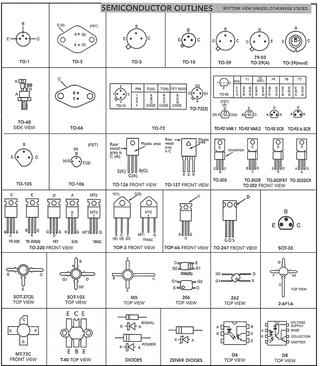
Illustrative reference to semiconductors; metadata does not identify specific devices or materials.
Credit: Nimal udayanga 12 · CC BY-SA 4.0 · sourceResized and converted to WebP; uncropped.
1. Scientific foundations and major semiconductor technologies
A semiconductor is a material whose electrical conductivity lies between that of a conductor and an insulator and can be controlled through doping, electric fields, temperature or light. Its relatively small energy band gap allows charge carriers to be generated or manipulated under suitable conditions. Silicon dominates because it is abundant, supports a useful native oxide and benefits from a mature manufacturing ecosystem.
Doping introduces controlled impurities into a semiconductor. Donor impurities produce n-type material with electrons as majority carriers, while acceptor impurities produce p-type material with holes as majority carriers. Bringing these regions together creates a p–n junction, fundamental to diodes, solar cells and many electronic devices. Transistors act as switches or amplifiers; integrated circuits combine large numbers of components on a small substrate.
Semiconductor products include logic chips that process information, memory chips that store it, analogue chips that handle continuous signals, and power devices that manage electrical energy. Microcontrollers integrate processing, memory and interfaces for embedded systems. Sensors translate physical conditions into electrical signals. Silicon carbide and gallium nitride, both wide-band-gap materials, can improve performance in electric-vehicle power electronics, charging systems, communications and renewable-energy equipment.
Smaller manufacturing nodes can improve transistor density, performance and energy efficiency, but are not essential for every application. Automotive, industrial and power-management systems frequently rely on mature nodes because reliability, voltage tolerance, cost and long product life matter more than maximum density. Thus, semiconductor capability should not be assessed only by the smallest node a country can manufacture.
Timeline
1947
The transistor was demonstrated at Bell Labs, establishing a foundation for modern solid-state electronics.
1958–1959
Jack Kilby and Robert Noyce developed pioneering integrated-circuit approaches.
December 2021
India approved the ₹76,000-crore semiconductor and display ecosystem programme.
September 2022
India modified the programme, introducing 50% project-cost fiscal support for semiconductor fabs across technology nodes.
February 2024
The Union Cabinet approved semiconductor projects at Dholera, Morigaon and Sanand.
2. Value chain, manufacturing and global interdependence
The semiconductor value chain begins with product architecture, intellectual-property blocks and chip design using electronic design automation software. Designs undergo verification before being converted into manufacturing instructions. A fabrication plant, or fab, repeatedly deposits, patterns, etches and modifies materials on wafers. Photolithography transfers patterns using light; extreme ultraviolet lithography is used in some advanced processes, while many established processes use other lithographic technologies.
After fabrication, wafers are tested and separated into individual dies. Assembly, packaging and testing provide electrical connections, mechanical protection and heat dissipation while screening defective devices. Advanced packaging connects multiple dies or chiplets within a package, improving functionality without relying exclusively on transistor miniaturisation. Consequently, packaging is increasingly a source of technological differentiation rather than merely a low-value final operation.
Business models differ. Fabless firms design chips but outsource manufacturing; foundries manufacture chips for other firms; integrated device manufacturers undertake both design and production. Outsourced semiconductor assembly and test firms specialise in downstream operations. ATMP refers to assembly, testing, marking and packaging, a closely related set of activities.
No country controls every segment efficiently. Taiwan has a major role in advanced contract manufacturing, South Korea in memory, the United States in design and key software, the Netherlands in advanced lithography equipment, and Japan in several materials and equipment categories. These specialisations create efficiencies but also concentrated dependencies. Capital intensity, process complexity, intellectual property and the difficulty of achieving high production yields create substantial entry barriers.
From chip concept to electronic product
- 1. Define application requirements and chip architecture
- 2. Design and verify circuits using specialised software
- 3. Fabricate circuits on semiconductor wafers
- 4. Probe wafers and separate individual dies
- 5. Package devices and conduct final testing
- 6. Integrate qualified chips into electronic systems
3. Strategic and societal applications
Semiconductors enable artificial intelligence, cloud computing, mobile networks, satellites, navigation, radar and secure communications. Dependence on imported chips can expose strategic sectors to supply disruption, export restrictions or compromised procurement channels. However, domestic fabrication alone cannot ensure security: trusted designs, secure firmware, traceable sourcing, testing and cybersecurity across the equipment lifecycle are equally important.
Their societal applications are extensive. Medical imaging and diagnostic equipment use specialised processors and sensors; agricultural systems use chips for soil monitoring, irrigation and remote sensing; digital payments and identity systems depend on secure computing infrastructure. Smart meters, grid controls, solar inverters and electric vehicles rely on power electronics. Affordable and reliable semiconductor access therefore supports public-service delivery, productivity and decarbonisation.
The pandemic-era chip shortage demonstrated that disruption in a specialised component can constrain entire industries. Automobile production was affected even where steel, labour and assembly capacity were available. Demand forecasting, inventory practices and limited substitutability intensified the problem. Meanwhile, subsidies, export controls and national-security screening have made semiconductor supply chains a central arena of industrial policy and geopolitical competition.
| Activity | Principal output | Critical requirement |
|---|---|---|
| Design | Chip architecture and verified circuit layout | Engineering talent, design software and intellectual property |
| Wafer fabrication | Electronic circuits formed on wafers | Process expertise, equipment, utilities and high yields |
| Assembly and packaging | Protected and interconnected dies | Packaging technology and thermal management |
| Testing | Devices screened for performance and reliability | Test equipment, coverage and quality assurance |
| Materials and equipment | Wafers, chemicals, gases and production tools | Extreme purity, precision and dependable supply |
4. India’s semiconductor strategy and emerging ecosystem
India has a substantial semiconductor design and engineering talent base, but commercial wafer-fabrication capacity remains limited relative to its electronics market. Existing institutions, including the Semi-Conductor Laboratory at Mohali, provide capabilities relevant to strategic and specialised requirements. The policy objective is to deepen domestic value addition rather than treat final electronics assembly as equivalent to semiconductor self-reliance.
The December 2021 semiconductor and display programme established a ₹76,000-crore policy envelope. Under the modified programme approved in 2022, eligible semiconductor fabs can receive fiscal support of 50% of project cost. Support for eligible compound-semiconductor, sensor, discrete-semiconductor and ATMP/OSAT facilities is structured around 50% of capital expenditure. These categories should not be conflated with identical reimbursement rules for every project.
India Semiconductor Mission supports ecosystem development and project appraisal. The Design Linked Incentive scheme seeks to strengthen domestic chip-design enterprises through financial and infrastructure support. The Chips to Startup programme supports specialised manpower development. Electronics-manufacturing incentives and demand from telecommunications, vehicles and energy systems can complement semiconductor policy, but cannot substitute for process expertise and sustained research.
Approved projects illustrate a multi-segment approach. In February 2024, the Union Cabinet approved a Tata Electronics fab at Dholera, Gujarat, in partnership with Taiwan’s PSMC; a Tata assembly and testing facility at Morigaon, Assam; and a CG Power-led unit at Sanand, Gujarat. Micron’s Sanand project, announced in 2023, concerns assembly and testing rather than wafer fabrication. Announced investments, approved capacity, construction milestones and commercial output must be distinguished.
5. Implementation challenges and policy priorities
A competitive ecosystem requires uninterrupted high-quality electricity, ultrapure water, cleanrooms, specialty gases, chemicals and dependable logistics. Fabs also require experienced process engineers and technicians capable of improving yield. High upfront expenditure, rapid technological change and cyclical chip prices create commercial risks. Subsidies may attract initial investment but cannot independently generate customer confidence, operational discipline or long-term competitiveness.
Environmental governance is essential. Manufacturing consumes substantial energy and water and uses hazardous chemicals; some process gases have high global-warming potential. Water recycling, wastewater treatment, emissions abatement, renewable power and transparent resource planning should accompany industrial development. Semiconductor manufacturing waste and end-of-life electronic waste are distinct issues requiring coordinated but different regulatory responses.
India should pursue selective technological depth with diversified international partnerships rather than complete autarky. Priorities include commercially viable mature-node manufacturing, power semiconductors, advanced packaging and domestic design intellectual property. Support should be linked to verifiable milestones, skills transfer, supplier development and market demand. University–industry collaboration, access to prototyping facilities and predictable policy can help Indian firms move from design services towards globally competitive semiconductor products.
Semiconductors: From Material Properties to Strategic Capability
Semiconductors are materials whose electrical conductivity can be controlled through doping, electric fields, temperature or light. This controllability enables devices such as diodes and transistors, which rectify current, switch signals or amplify them. Silicon dominates many applications, while compound semiconductors serve specialised needs, including high-frequency communications and power electronics. The supplied metadata identifies only “semiconductor outlines”; it cannot establish a particular material, device architecture, manufacturing process or performance level.
For India, semiconductor capability requires more than a fabrication plant. The value chain spans chip design, design software, intellectual property, wafer fabrication, assembly, testing and packaging, alongside specialised materials and equipment. Fabrication demands reliable electricity, ultrapure water, contamination control and skilled personnel; packaging and testing also require sophisticated engineering. Strategic resilience therefore means addressing critical dependencies and building trusted supply relationships, rather than assuming complete domestic self-sufficiency. Policy evaluation should consider commercial viability, infrastructure, skills, environmental management and sustained technological upgrading, not merely announced investments.
- Distinguish material, device and product: silicon is a semiconductor material; a transistor is a device; an integrated circuit combines interconnected devices.
- A smaller process-node label does not automatically mean the best chip for every use. Automotive, industrial and power applications may prioritise reliability, voltage tolerance and cost.
- Design strength does not equal manufacturing capacity. Assess fabrication and assembly, testing and packaging separately; this image metadata provides no evidence of either capability.
Real-world case studies
Pandemic-era automotive semiconductor shortage
During 2020–2022, disrupted production and shifts in electronics demand contributed to severe automotive chip shortages. Vehicle manufacturers could not readily replace qualified microcontrollers and other components with alternative chips. The episode illustrates the importance of mature nodes, supplier visibility, diversified procurement and realistic resilience planning.
Dholera semiconductor fab
The Tata Electronics–PSMC project approved in February 2024 envisaged investment of about ₹91,000 crore and capacity of 50,000 wafer starts per month. Planned products included power-management chips and applications using 28 nm technology. It illustrates India’s attempt to combine public support with international process expertise. These approval-stage figures represent planned investment and capacity, not proof of achieved output.
Previous year questions
No source-linked PYQ is available here yet. Use the practice questions below.
Practice questions
Practice MCQ 1
Consider the following statements: 1. Doping can modify a semiconductor’s electrical conductivity. 2. All automotive chips require the most advanced manufacturing nodes. 3. Gallium nitride is a wide-band-gap semiconductor. Which statements are correct?
- A. 1 and 2 only
- B. 1 and 3 only
- C. 2 and 3 only
- D. 1, 2 and 3
Practice MCQ 2
Which statement correctly distinguishes semiconductor business models?
- A. A fabless company necessarily owns wafer-fabrication plants.
- B. A foundry primarily manufactures chips designed by customers.
- C. An OSAT company exclusively develops chip-design software.
- D. An integrated device manufacturer undertakes only packaging.
Practice MCQ 3
Why can advanced packaging improve semiconductor-system performance?
- A. It eliminates the need for semiconductor fabrication.
- B. It makes all chip designs interchangeable.
- C. It enables close integration of multiple dies or chiplets.
- D. It removes the need for heat management.
Mains practice · Semiconductor self-reliance requires an ecosystem, not merely fabrication plants. Examine this statement in the context of India’s technological and economic security. Suggest policy priorities. Answer in 250 words.
- Explain the distributed value chain: design, software, materials, equipment, fabrication, packaging and testing.
- Connect semiconductor access with defence, digital infrastructure, mobility, health and energy security.
- Assess India’s design strengths alongside manufacturing, supplier and process-skill gaps.
- Discuss India Semiconductor Mission, fiscal support, design incentives and skills programmes.
- Recommend milestone-linked incentives, commercially viable technology choices, supplier development and research collaboration.
- Address resource efficiency and diversified international partnerships; distinguish resilience from complete autarky.
Further reading
- NCERT, Physics Part II, Class XII: Semiconductor Electronics: Materials, Devices and Simple Circuits.
- Ministry of Electronics and Information Technology: semiconductor programme documents and annual reports, meity.gov.in.
- India Semiconductor Mission: scheme guidelines and official project information, ism.gov.in.
- Press Information Bureau: Cabinet releases of 15 December 2021, 21 September 2022 and 29 February 2024.
- C-DAC: official Design Linked Incentive scheme and Chips to Startup programme resources.
- https://commons.wikimedia.org/wiki/File:Semiconductor_outlines.jpg
Preparing for UPSC Civil Services? Get classroom teaching, answer-writing evaluation and mentorship at Pragnya IAS Academy, Ashok Nagar — see why aspirants choose us for IAS coaching in Hyderabad.